In this 8051 tutorial, we will learn the 8051 Pin Diagram and 8051 microcontroller Pin Description. Like other microcontrollers 8051 pin diagram also describes the functionality of each pin and help you to identify the ports and other pins.
Pins of 8051 Microcontroller
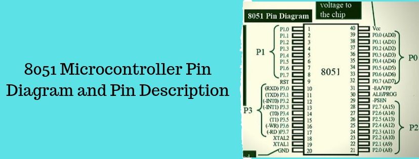
The Below image describes the Pin Diagram of 8051 with respect to 40 pins. In 8051 Pin Diagram, you can see that it has 4 ports P0, P1, P2, and P3 and each port has 8 pin. The below, 8051 Pin Diagram also describe the remaining 8 pins.
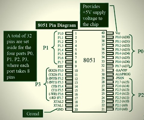
Explanation of 8051 pin diagram
Pins 1 – 8:
Port1 uses the Pins 1 to 8. Each pin is bidirectional Input /Output with internal pull – up resistors.
Pin 9:
It is a reset input Pin which used to reset the 8051 microcontrollers. It is an active HIGH Pin i.e. if we apply a high pulse to this pin, the microcontroller will reset and terminate all activities.
Note: All value of the register will be lost after activating a power-on reset.
Pins 10-17:
Port3 uses the Pins 10 to 17. Each pin is bidirectional Input /Output with internal pull – up resistors. Besides the Input /Output, each pin has some special functionality. In the below table, I have described the other functionality of Port-3.
| PORT 3 Bit and Pin | Function | Description |
| P3.0 (10) | RXD | Serial Input |
| P3.1 (11) | TXD | Serial Output |
| P3.2 (12) |
INT0
|
External Interrupt 0 |
| P3.3 (13) |
INT1
|
External Interrupt 1 |
| P3.4 (14) | T0 | Timer 0 |
| P3.5 (15) | T1 | Timer 1 |
| P3.6 (16) |
WR
|
External Memory Write |
| P3.7 (17) |
RD
|
External Memory Read |
Pins 18 & 19:
Pin 18 and 19 are used for interfacing an external crystal oscillator to get the system clock. We should use the ceramic capacitor with an external crystal oscillator.
Pin 20 (GND):
Pin 20 is the Ground Pin of the 8051 Microcontroller.
Pins 21 -28:
Port2 uses the Pins 21 to 28. Each pin is bidirectional Input /Output with internal pull – up resistors. Besides the Input /Output, when external memory is interfaced, PORT 2 pins act as the higher-order address byte.
Pin 29 (PSEN):
Pin 29 is the Program Store Enable Pin (PSEN). It is an output pin and using this pin, external Program Memory can be read.
Pin 30 (ALE/PROG):
Pin 30 is the Address Latch Enable Pin. It is an output pin and using this Pin, external address can be separated from data (as they are multiplexed by 8051).
Pin 31 (EA/VPP):
Pin 31 is the External Access Enable Pin i.e. allows external Program Memory. It is an input pin and must be connected from VCC or GND. If you want to access the code from external program memory, it must be connected with GND. If you want to use on-chip memory, it must be high (connected with VCC).
Pins 32–39:
Port0 uses the Pins 32 to 39. Each pin is bidirectional Input /Output but without internal pull – up resistors. So we need to use an external pull-up before using Port0 as Input /Output.
Pin 40 (VCC):
Pin 40 is the power supply pin of the 8051 Microcontroller. It should be +5V.
Recommended Post
- Led blinking program in c for 8051.
- Interfacing of switch and led using the 8051
- Interfacing of Relay with 8051 microcontroller
- Moving message display on LCD using 8051
- LCD 4-bit mode c code for 8051.
- Create LCD custom characters for 16×2 alphanumeric LCD
- Interfacing of keypad with 8051
- Electronic digital lock using the 8051
- Interfacing of EEPROM with 8051 microcontrollers using I2C
- Embedded c interview questions.
- 8051 Architecture.