Clock configuration is one of the most critical aspects of any firmware design. A stable and well-optimized clock tree ensures accurate timing, reliable peripheral communication, and consistent real-time performance across the system. In embedded systems, clock instability can directly lead to system failure.
In this article, I will explain the clock system and its configuration procedure for the STM32H5 microcontroller in detail. Although the example focuses on the STM32H5 series, the overall approach is largely similar across most STM32 families and can be adapted with minor adjustments depending on the specific clock circuitry used.
Microcontroller System Clock:
In any microcontroller, the system clock plays a role as vital as the heartbeat in a living organism. It keeps every digital element alive and synchronized. In the silicon world, this clock governs how instructions flow, how peripherals operate, and how time-sensitive operations are executed.
In the STM32H5 series, this heartbeat originates from the Reset and Clock Control (RCC) peripheral, which acts as the central hub for generating, selecting, and distributing clocks. The Arm® Cortex®-M processor and every on-chip peripheral like including timers, communication interfaces, and memory buses — rely on these RCC-managed clock sources to function correctly.
A well-designed clock configuration ensures optimal performance, power efficiency, and timing stability, while a poor configuration can lead to unpredictable behavior, jitter, or even system instability.
Reset and Clock Control (RCC):
The Reset and Clock Control (RCC) peripheral is one of the most crucial components in any STM32 microcontroller. It manages the different resets and generates the clocks for the bus and peripherals.
RCC provides a centralized mechanism to manage clock sources, prescalers, and reset signals across the system. Every peripheral, CPU core, and bus in the MCU depends on the RCC to operate at the desired frequency. The configuration and number of available clocks may vary slightly between STM32 families (F0, F1, H5, G4, etc.), but the overall structure remains consistent.
Clock Sources:
The STM32 RCC (Reset and Clock Control) module provides several clock sources that can be used to generate the system clock (SYSCLK).
Four different clock sources can be used to drive the system clock (SYSCLK):
- HSI: high-speed internal up to 64 MHz RC oscillator clock.
- CSI: low power internal RC oscillator clock.
- HSE: high-speed external crystal or clock, from 4 to 50 MHz.
- PLL1 clock

The device has the following additional clock sources:
- LSI: 32 kHz low-speed internal RC that drives the independent watchdog and optionally the RTC used for auto-wakeup from Stop and Standby modes.
- LSE: 32.768 kHz low-speed external crystal or clock that optionally drives the real-time clock (rtc_ck).
- HSI48: internal 48 MHz RC that potentially drives the USB FS and the RNG.
- PLL2 and PLL3 clocks.

Note: Each clock source can be switched on or off independently when it is not used, to optimize power consumption.
Phase-Locked Loops (PLLs):
The STM32H5 integrates three fully independent Phase-Locked Loops (PLL1, PLL2, and PLL3) within its RCC (Reset and Clock Control) unit. Each PLL can generate up to three precise output clocks (P, Q, and R) used by the CPU and various peripherals.
PLL1 typically drives the system clock (SYSCLK), while PLL2 and PLL3 are dedicated to generating peripheral kernel clocks for interfaces such as USB, FDCAN, SAI, and SDMMC.
Each PLL includes a Voltage-Controlled Oscillator (VCO) supporting both wide-range (for high-speed operation) and low-range (for low-power or audio applications) modes.
The reference input frequency (1–16 MHz) is divided by M, multiplied by N, and then divided by output prescalers P, Q, and R to generate the desired clock frequencies.
PLLs can operate in either integer or fractional mode, the latter enabled by a 13-bit sigma-delta modulator that allows ultra-fine frequency tuning down to 0.3 ppm without jitter spikes or frequency overshoot.
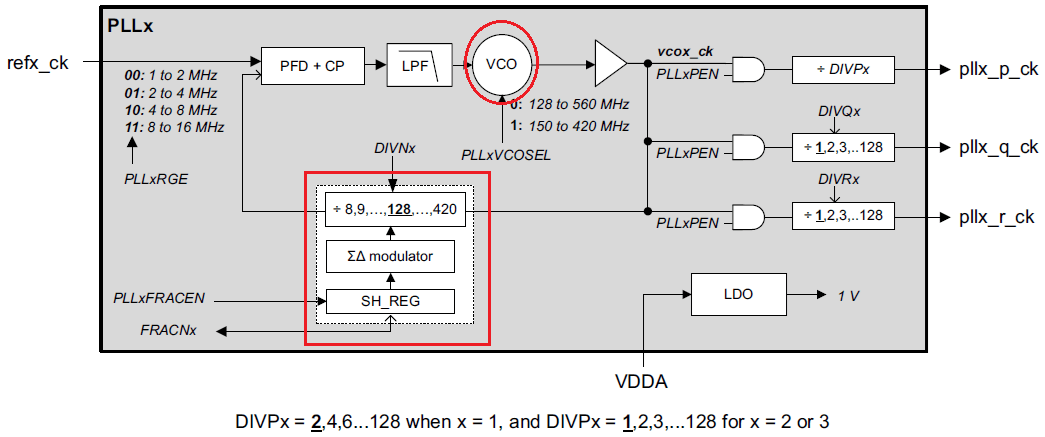
In STM32 microcontrollers, the configuration of Phase-Locked Loops (PLLs) is managed through a set of dedicated RCC (Reset and Clock Control) registers. These registers define the PLL’s input source, multiplication and division factors, operational mode, and control status.
- RCC_PLLxDIVR: Sets the input divider (M), multiplication factor (N), and output dividers (P, Q, R) for the PLL.
- RCC_PLLxFRACR: Enables and configures fractional mode for ultra-fine frequency tuning.
- RCC_PLLCFGR: Selects the PLL input source, VCO range, and other operational parameters.
- RCC_CR: Controls the PLL enable/disable state and monitors the PLL lock status.
To activate a PLL:
- Set the PLLxON bit in RCC_CR.
- Wait for the PLLxRDY flag to be set, indicating that the PLL has locked and the output frequency is stable.
⚠️ Note: Once a PLL is active, parameters such as DIVN, PLLxRGE, VCOSEL, and output dividers (DIVP, DIVQ, DIVR) must not be modified. Changing these while the PLL is running can lead to unstable or undefined clock behavior.
Example: Configuring PLL1 to Generate 400 MHz SYSCLK from 8 MHz HSE
The PLL can multiply the frequency of HSI, HSE or CSI to achieve higher clock frequencies. It involves:
- Selecting the input source (HSI, HSE or CSI).
- Setting the multiplication factor
- Configuring dividers.
In this example we are using an external 8 MHz crystal oscillator (HSE) and want to configure the system clock (SYSCLK) to 400 MHz using PLL1.
Step 1: PLL Frequency Formula
Each PLL in STM32H5 follows this equation:
FVCO = (FIN/M)×N
FOUTx= FVCO/ DIVx
Where:
- FIN = input frequency (HSE, HSI, or CSI)
- M = input prescaler (1–63)
- N = multiplication factor (4–512)
- DIVx = output divider (2–128) for P, Q, or R outputs
The SYSCLK is derived from PLL1_P, PLL1_Q, or PLL1_R depending on selection.
Note: DIVPx ranges from 2–128 for PLL1 and 1–128 for PLL2/PLL3, while DIVQx and DIVRx always range from 1–128, defining the output dividers for the respective P, Q, and R clocks.
Step 2: Choose PLL Parameters
We want SYSCLK = 400 MHz using HSE = 8 MHz.
Choose:
- PLL1_M = 2 (Input pre scalar)
- PLL1_N = 100 (multiplication factor)
- PLL1_P = 2 (Post divider)
Now:
- FVCO = (8MHz/2) × 100=400MHz
- FPLL1_P=(400MHz/2) = 200MHz
- FPLL1_R=(400MHz/1) = 400MHz
We can select PLL1_R output as the SYSCLK source to achieve 400 MHz CPU clock.
Step 3: PLL Configuration using HAL
void SystemClock_Config(void)
{
    RCC_OscInitTypeDef RCC_OscInitStruct = {0};   // Structure for oscillator configuration
    RCC_ClkInitTypeDef RCC_ClkInitStruct = {0};   // Structure for bus clock configuration

    /*----------------------------------------------------------*/
    /* 0. Enable PWR Clock and Configure Voltage Scaling        */
    /*----------------------------------------------------------*/

    // Enable power control clock
    __HAL_RCC_PWR_CLK_ENABLE();

    // Set regulator output voltage to Scale 0 (highest performance for 400 MHz SYSCLK)
    __HAL_PWR_VOLTAGESCALING_CONFIG(PWR_REGULATOR_VOLTAGE_SCALE0);

    // Wait until voltage scaling is ready
    while (!__HAL_PWR_GET_FLAG(PWR_FLAG_VOSRDY)) {}

    /*----------------------------------------------------------*/
    /* 1. Configure HSE (External Oscillator) and Enable PLL1   */
    /*----------------------------------------------------------*/

    // Select external crystal (HSE)
    RCC_OscInitStruct.OscillatorType = RCC_OSCILLATORTYPE_HSE;

    // Turn ON the HSE oscillator
    RCC_OscInitStruct.HSEState = RCC_HSE_ON;

    // Enable PLL1
    RCC_OscInitStruct.PLL.PLLState = RCC_PLL_ON;

    // Select HSE as PLL input source
    RCC_OscInitStruct.PLL.PLLSource = RCC_PLLSOURCE_HSE;

    // PLL input divider: 8 MHz / 2 = 4 MHz
    RCC_OscInitStruct.PLL.PLLM = 2;

    // PLL multiplier: 4 MHz × 100 = 400 MHz (VCO frequency)
    RCC_OscInitStruct.PLL.PLLN = 100;

    // PLL1_P output = 400 / 2 = 200 MHz (optional peripheral clock)
    RCC_OscInitStruct.PLL.PLLP = 2;

    // PLL1_Q output = 400 / 4 = 100 MHz (optional peripheral clock)
    RCC_OscInitStruct.PLL.PLLQ = 4;

    // PLL1_R output = 400 / 1 = 400 MHz → used as SYSCLK
    RCC_OscInitStruct.PLL.PLLR = 1;

    // PLL input frequency range: 1–2 MHz
    RCC_OscInitStruct.PLL.PLLRGE = RCC_PLLVCIRANGE_1;

    // Select medium VCO range (for ~400 MHz operation)
    RCC_OscInitStruct.PLL.PLLVCOSEL = RCC_PLLVCOMEDIUM;

    // Disable fractional mode (integer multiplication)
    RCC_OscInitStruct.PLL.PLLFRACN = 0;

    // Apply oscillator and PLL configuration
    if (HAL_RCC_OscConfig(&RCC_OscInitStruct) != HAL_OK)
    {
        Error_Handler();  // Handle configuration error
    }

    /*----------------------------------------------------------*/
    /* 2. Configure CPU, AHB, and APB Bus Clocks                */
    /*----------------------------------------------------------*/

    // Configure SYSCLK, HCLK, PCLK1, and PCLK2
    RCC_ClkInitStruct.ClockType = RCC_CLOCKTYPE_SYSCLK |
                                  RCC_CLOCKTYPE_HCLK   |
                                  RCC_CLOCKTYPE_PCLK1  |
                                  RCC_CLOCKTYPE_PCLK2;

    // Select PLL1_R as system clock source (400 MHz)
    RCC_ClkInitStruct.SYSCLKSource = RCC_SYSCLKSOURCE_PLL1;

    // AHB clock = SYSCLK / 1 → 400 MHz
    RCC_ClkInitStruct.AHBCLKDivider = RCC_SYSCLK_DIV1;

    // APB1 clock = HCLK / 2 → 200 MHz
    RCC_ClkInitStruct.APB1CLKDivider = RCC_HCLK_DIV2;

    // APB2 clock = HCLK / 2 → 200 MHz
    RCC_ClkInitStruct.APB2CLKDivider = RCC_HCLK_DIV2;

    // Apply bus clock configuration and set Flash latency
    if (HAL_RCC_ClockConfig(&RCC_ClkInitStruct, FLASH_LATENCY_5) != HAL_OK)
    {
        Error_Handler();  // Handle configuration error
    }

    /*----------------------------------------------------------*/
    /* 3. Frequency Summary (for reference & verification)      */
    /*----------------------------------------------------------*/
    /*
        HSE Frequency      = 8  MHz
        PLL Input (M)      = 4  MHz  (8 / 2)
        PLL VCO            = 400 MHz (4 × 100)
        PLL1_P Output      = 200 MHz
        PLL1_Q Output      = 100 MHz
        PLL1_R Output      = 400 MHz (used as SYSCLK)
        AHB Clock (HCLK)   = 400 MHz
        APB1 Clock (PCLK1) = 200 MHz
        APB2 Clock (PCLK2) = 200 MHz
        Flash Latency      = 5 WS
        Voltage Scaling    = Scale 0 (highest performance)
    */
}
Note: When operating at high CPU frequencies, Flash memory access may require wait states to ensure timing integrity. Always configure Flash latency appropriately before increasing the system clock speed. Failing to do so can lead to incorrect instruction fetches or data corruption.
Clock Output Generation (MCO1 / MCO2 / LSCO):
The STM32H5 series provides two microcontroller clock output pins (MCO1 and MCO2), which allow selected internal clocks to be routed to external pins. These outputs are useful for debugging, measuring, or providing clocks to other components.
- Clock source: Each MCO pin can output a selectable clock from internal sources (SYSCLK, HSI, HSE, PLLs, etc.).
- Prescaler: The output can be divided using a configurable prescaler to reduce the frequency.
Configuration registers:
- MCO1 → MCO1[2:0] and MCO1PRE[3:0] (RCC_CFGR1)
- MCO2 → MCO2[2:0] and MCO2PRE[3:0] (RCC_CFGR1)
- GPIO: MCO pins must be configured in Alternate Function mode.
Limitations: Output frequency must not exceed the pin’s maximum rated speed (see datasheet).
Example:
LL_RCC_ConfigMCO(LL_RCC_MCO1SOURCE_SYSCLK, LL_RCC_MCO1_DIV_4); // SYSCLK/4 on MCO1
LSCO (Low-Speed Clock Output)
- Purpose: Outputs a low-speed clock (LSI or LSE) on the external LSCO pin.
- Availability: Works in Stop mode, but not in Standby or VBAT modes.
- Control:
- LSCOSEL → selects LSI or LSE
- LSCOEN → enables LSCO (RCC_BDCR)
- Pin requirement: LSCO pin remains in default state, no alternate function needed.
Bus Architecture and Clock Domains:
The STM32H5 series microcontrollers implement the AMBA (Advanced Microcontroller Bus Architecture) defined by ARM, which standardizes communication between the processor core, memory, and peripherals.
This series use the two bus interfaces, Advanced High-performance Bus (AHB) and the Advanced Peripheral Bus (APB).

1. Advanced High-performance Bus (AHB)
The AHB forms the high-speed backbone of the STM32H5 architecture. It interconnects the Cortex-M33 core, Flash memory, SRAM, DMA, and other high-performance peripherals.
The AHB domain is driven by the HCLK (AHB Clock), which is derived from the system clock (SYSCLK) through a programmable prescaler.
Key characteristics:
- Provides high bandwidth for core and memory access.
- Supports burst transfers and pipelined operations for faster execution.
- Serves as the parent clock source for lower-speed peripheral buses.
Clock signal:
HCLK → Drives the CPU, memory interface, and DMA.
2. Advanced Peripheral Bus (APB)
The APB is designed for low-power and low-speed peripherals. In STM32H5, this bus type is split into three domains — APB1, APB2, and APB3, each clocked independently through prescalers derived from HCLK. This division allows selective power control and performance optimization for different groups of peripherals.
APB1 Bus:
- Clock: PCLK1
- Source: Derived from HCLK via a prescaler.
- Used by: Low-speed peripherals such as TIM2–TIM7, USART2–USART5, I2C1–I2C3, SPI2, and LPUART1.
- Purpose: Provides slower clocking for general-purpose and communication peripherals to reduce power consumption.
APB2 Bus:
- Clock: PCLK2
- Source: Derived from HCLK via a prescaler.
- Used by: High-speed peripherals like TIM1, SPI1, USART1, and ADC.
- Purpose: Supports peripherals that require faster data exchange or tighter timing.
APB3 Bus:
- Clock: PCLK3
- Source: Derived from HCLK via a prescaler.
- Used by: System-level peripherals such as SYSCFG, PWR, EXTI, and RTC.
- Purpose: Dedicated for system configuration and control peripherals, separating them from the main data and peripheral traffic.
Peripheral Clock Gating and Autonomous Mode:
Autonomous mode allows selected peripherals to continue operating, exchanging data, and even waking up the CPU — all while the rest of the system remains in low-power mode. This ensures energy efficiency without compromising responsiveness or real-time performance.
In STM32H5 microcontrollers, each peripheral’s clock is managed using enable (EN) bits located in the RCC_AHBxENR and RCC_APBxENR registers.
- When an EN bit is set, the corresponding peripheral receives its clock and becomes fully operational.
- When the EN bit is cleared, the clock to that peripheral is disabled, and its registers become inaccessible.
⚠️ Important: If a peripheral’s clock is not active, any attempt to read from or write to its registers will fail. The peripheral must be clocked to allow register access.
Caution: Just after enabling the clock for a peripheral, the software must wait for these 2 clock cycles before accessing the peripheral registers.
How to Check the Current Clock Frequencies:
It is essential to ensure your STM32 clock configuration is correctly set up to avoid timing issues and peripheral malfunctions. You can use HAL-provided functions such as HAL_RCC_GetSysClockFreq(), HAL_RCC_GetHCLKFreq(), HAL_RCC_GetPCLK1Freq(), and HAL_RCC_GetPCLK2Freq() to read and verify the current system and bus clock frequencies during runtime.
These functions are especially useful for debugging, performance tuning, and validating dynamic clock changes.
Consider the below example code,
void printClockFrequencies()
{
    uint32_t sysclk = HAL_RCC_GetSysClockFreq();
    uint32_t hclk   = HAL_RCC_GetHCLKFreq();
    uint32_t pclk1  = HAL_RCC_GetPCLK1Freq();
    uint32_t pclk2  = HAL_RCC_GetPCLK2Freq();

    printf("System Clock (SYSCLK): %lu Hz\r\n", sysclk);
    printf("AHB Clock     (HCLK):   %lu Hz\r\n", hclk);
    printf("APB1 Clock    (PCLK1):  %lu Hz\r\n", pclk1);
    printf("APB2 Clock    (PCLK2):  %lu Hz\r\n", pclk2);
}