Interfacing an external flash memory with a microcontroller is a common task in embedded systems to minimize unnecessary access to the MCU’s internal flash. Embedded firmware developers often use external flash for data logging, firmware storage, and IoT applications.
External flash memory often includes communication interfaces such as I2C, SPI, or QSPI. System architects ensure the chosen microcontroller supports all required interfaces to communicate effectively with other components in the product. However, incorporating multiple hardware peripheral interfaces can increase the microcontroller’s cost, potentially exceeding the BOM (Bill of Materials) budget. In such cases, cost-effective techniques like bit-banging can serve as viable alternatives.
In this blog post, I will explain how to interface a Macronix external flash with an STM32 microcontroller using bit-banging. Although both devices typically include dedicated QSPI (Quad Serial Peripheral Interface) hardware peripherals to simplify this process, we will use bit-banging—a software-driven technique that emulates QSPI communication using general-purpose I/O (GPIO) pins—for educational purposes.
In this QSPI bit-banging tutorial, we’ll guide you through the process of interfacing external flash with an STM32 using bit-banging, complete with code examples and practical tips.
What is QSPI?
A Quad Serial Peripheral Interface is an extension of the standard SPI protocol. It supports a wide range of external serial memories, including serial NOR flash, NAND flash, PSRAM, HyperRAM, and HyperFlash.
What is QSPI Bit Banging?
Bit banging refers to the technique of generating a series of pulses or signals entirely in firmware to emulate a communication protocol (like SPI, I2C, or UART), instead of relying on a piece of hardware inside the microcontroller.
It involves manually toggling GPIO pins to create the necessary timing and sequence of bits, giving the firmware full control over the signal but often at the cost of higher CPU usage and less precise timing compared to hardware-based solutions.
Now let’s talk about the QSPI bit-banging.
QSPI bit-banging is a technique where firmware manually controls GPIO pins to mimic the QSPI protocol, which is used to communicate with external flash memory. Unlike standard SPI, QSPI uses four data lines (IO0–IO3) for faster data transfer, making it ideal for high-speed applications. However, without a dedicated QSPI peripheral, you can use firmware bit-banging to toggle pins according to the QSPI timing requirements.
QSPI bit-banging is particularly useful when:
- Your microcontroller lacks a QSPI peripheral.
- You need to use non-standard pins due to pin conflicts.
- You’re working with a custom or proprietary protocol.
- Cost constraints favor simpler microcontrollers.
Step-by-Step QSPI Interfacing Tutorial:
Now let’s dive into the process of interfacing external flash with QSPI using bit banging. I am using here STM32H5xxx (you can use any generic microcontroller, e.g., Rx, AVR, or PIC) and assume a common external flash chip like the Macronix series or, Winbond series.
So let’s see the steps for QSPI interfacing.
Step 1: Understand QSPI Protocol Basics:
QSPI operates similarly to SPI but uses four data lines for quad-mode transfers. Key signals include:
- SCLK: Serial clock.
- CS: Chip select (active low).
- IO0–IO3: Four bidirectional data lines for quad I/O mode.
The external flash typically supports commands (JEDEC Flash commands) like:
- JEDEC ID (0x9F): Reads manufacturer and device ID.
- Read Data (0x03 or 0x0B): Read data from a specific address.
- Write Enable (0x06): Enable writing to the flash.
- Page Program (0x02): Write data to a specific page.
- Sector Erase (0x20): Erase a sector before writing.
You need to toggle the above-mentioned pins for bit banging to send commands, addresses, and data.
Step 2: Hardware Setup:
Interface the external flash memory with your microcontroller.
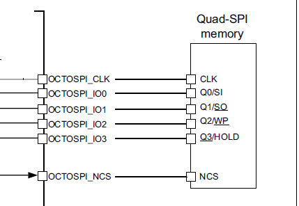
You can choose any port or pin for the connection, but for this example (Single SPI Mode), I will use the following pins:
- CS: GPIO pin (e.g., PA11).
- SCLK: GPIO pin (e.g., PA2).
- IO0 (MOSI): GPIO pin (e.g., PA1).
- IO1 (MISO): GPIO pin (e.g., PA0).
- IO2 (WP): GPIO pin (e.g., PA7).
- IO3 (RESET): GPIO pin (e.g., PA6).
- VCC/GND: Power the flash chip (typically in range 1.65 – 3.6V, you need to check your external flash data sheet).
Step 3: Initialize GPIO Pins
Before starting communication with the flash memory, it’s essential to configure the GPIOs used for bit banging. Each QSPI signal line should be set to either output or input mode as per its role during operation. I am using Single SPI Mode for bit-banging. Here is an example in C for a generic microcontroller.
Complete Code: Bare-Metal Bit-Banged QSPI Interface to Read JEDEC ID from External Flash:
Below is the complete bare-metal implementation of a bit-banged QSPI interface using GPIOs. This code reads the JEDEC ID from a QSPI Flash memory (e.g., Macronix MX25R6435F) without using HAL or any external libraries, making it ideal for learning or use in minimal embedded systems.
/**
 * @file main.c
 * @brief Bit-banged SPI communication with QSPI Flash using STM32H563.
 *
 * This example demonstrates bit-banged SPI communication with a QSPI flash device
 * using GPIO on the STM32H5 microcontroller. It includes initialization,
 * JEDEC ID read, sector erase, page program, and read operations.
 */

#include "stm32h563xx.h"

// === GPIO Pin Configuration Macros ===

#define CLK_PORT GPIOA /**< SPI Clock GPIO Port */
#define CLK_PIN 2      /**< SPI Clock Pin */

#define MOSI_PORT GPIOA /**< Master Out Slave In GPIO Port */
#define MOSI_PIN 1      /**< Master Out Slave In Pin */

#define MISO_PORT GPIOA /**< Master In Slave Out GPIO Port */
#define MISO_PIN 0      /**< Master In Slave Out Pin */

#define RESET_PORT GPIOA /**< Reset GPIO Port */
#define RESET_PIN 6      /**< Reset Pin */

#define WP_PORT GPIOA /**< Write Protect GPIO Port */
#define WP_PIN 7      /**< Write Protect Pin */

#define CS_PORT GPIOA /**< Chip Select GPIO Port */
#define CS_PIN 11     /**< Chip Select Pin */

// === GPIO Macros ===
/**
 * @brief Set GPIO pin high.
 */
#define GPIO_SET(port, pin) ((port)->BSRR = (1 << (pin)))

/**
 * @brief Set GPIO pin low.
 */
#define GPIO_CLR(port, pin) ((port)->BSRR = (1 << ((pin) + 16)))

/**
 * @brief Read GPIO pin value.
 * @return 1 if high, 0 if low.
 */
#define GPIO_READ(port, pin) (((port)->IDR >> (pin)) & 1)

/**
 * @brief Short delay using NOPs (for SPI timing).
 */
void delay_short(void)
{
   for (volatile int i = 0; i < 50; ++i)
      __NOP();
}

/**
 * @brief Send a byte via bit-banged SPI.
 * @param data Byte to send.
 */
void spi_send(uint8_t data)
{
   for (int i = 7; i >= 0; i--)
   {
      (data & (1 << i)) ? GPIO_SET(MOSI_PORT, MOSI_PIN) : GPIO_CLR(MOSI_PORT, MOSI_PIN);
      GPIO_SET(CLK_PORT, CLK_PIN);
      delay_short();
      GPIO_CLR(CLK_PORT, CLK_PIN);
      delay_short();
   }
}

/**
 * @brief Receive a byte via bit-banged SPI.
 * @return Received byte.
 */
uint8_t spi_receive(void)
{
   uint8_t result = 0;
   for (int i = 7; i >= 0; i--)
   {
      GPIO_SET(CLK_PORT, CLK_PIN);
      delay_short();
      result |= (GPIO_READ(MISO_PORT, MISO_PIN) << i);
      GPIO_CLR(CLK_PORT, CLK_PIN);
      delay_short();
   }
   return result;
}

/**
 * @brief Send Write Enable command to flash.
 */
void flash_write_enable(void)
{
   GPIO_CLR(CS_PORT, CS_PIN);
   spi_send(0x06); // Write Enable
   GPIO_SET(CS_PORT, CS_PIN);
}

/**
 * @brief Read the flash status register.
 * @return Status register value.
 */
uint8_t flash_read_status(void)
{
   GPIO_CLR(CS_PORT, CS_PIN);
   spi_send(0x05); // Read Status Register
   uint8_t status = spi_receive();
   GPIO_SET(CS_PORT, CS_PIN);
   return status;
}

/**
 * @brief Wait until flash is no longer busy.
 */
void flash_wait_busy(void)
{
   while (flash_read_status() & 0x01)
      ; // Wait until WIP = 0
}

/**
 * @brief Read JEDEC ID from flash.
 * @param[out] id Pointer to 3-byte array to store the ID.
 */
void flash_jedec_id(uint8_t* id)
{
   GPIO_CLR(CS_PORT, CS_PIN);
   spi_send(0x9F);
   id[0] = spi_receive(); // Manufacturer
   id[1] = spi_receive(); // Memory type
   id[2] = spi_receive(); // Capacity
   GPIO_SET(CS_PORT, CS_PIN);
}

/**
 * @brief Erase a 4KB sector at given address.
 * @param addr 24-bit sector address.
 */
void flash_erase_sector(uint32_t addr)
{
   flash_write_enable();

   GPIO_CLR(CS_PORT, CS_PIN);
   spi_send(0x20); // Sector Erase Command

   spi_send((addr >> 16) & 0xFF);
   spi_send((addr >> 8) & 0xFF);
   spi_send(addr & 0xFF);

   GPIO_SET(CS_PORT, CS_PIN);
}

/**
 * @brief Read data from flash memory.
 * @param addr 24-bit starting address.
 * @param[out] buf Destination buffer.
 * @param len Number of bytes to read.
 */
void flash_read(uint32_t addr, uint8_t* buf, uint32_t len)
{
   GPIO_CLR(CS_PORT, CS_PIN);
   spi_send(0x03); // Read command
   spi_send((addr >> 16) & 0xFF);
   spi_send((addr >> 8) & 0xFF);
   spi_send(addr & 0xFF);

   for (uint32_t i = 0; i < len; ++i)
      buf[i] = spi_receive();

   GPIO_SET(CS_PORT, CS_PIN);
}

/**
 * @brief Write a page (max 256 bytes) to flash memory.
 * @param addr 24-bit page-aligned address.
 * @param data Pointer to data buffer.
 * @param len Length in bytes (max 256).
 */
void flash_page_program(uint32_t addr, const uint8_t* data, uint32_t len)
{
   if (len > 256)
      return; // One page max

   flash_write_enable();

   GPIO_CLR(CS_PORT, CS_PIN);
   spi_send(0x02); // Page Program command
   spi_send((addr >> 16) & 0xFF);
   spi_send((addr >> 8) & 0xFF);
   spi_send(addr & 0xFF);

   for (uint32_t i = 0; i < len; ++i)
      spi_send(data[i]);

   GPIO_SET(CS_PORT, CS_PIN);

   flash_wait_busy(); // Wait for write to complete
}

/**
 * @brief Initialize GPIOs used for bit-banged SPI and flash control.
 */
void gpio_init(void)
{
   RCC->AHB2ENR |= RCC_AHB2ENR_GPIOAEN;

   // RESET, WP as output
   GPIOA->MODER &= ~((3 << (RESET_PIN * 2)) | (3 << (WP_PIN * 2)));
   GPIOA->MODER |= (1 << (RESET_PIN * 2)) | (1 << (WP_PIN * 2));

   // MISO as input with optional pull-up
   GPIOA->MODER &= ~(3 << (MISO_PIN * 2));
   GPIOA->PUPDR &= ~(3 << (MISO_PIN * 2));
   GPIOA->PUPDR |= (1 << (MISO_PIN * 2)); // Optional pull-up

   // MOSI, CLK as output
   GPIOA->MODER &= ~((3 << (MOSI_PIN * 2)) | (3 << (CLK_PIN * 2)));
   GPIOA->MODER |= (1 << (MOSI_PIN * 2)) | (1 << (CLK_PIN * 2));

   // CS as output
   GPIOA->MODER &= ~(3 << (CS_PIN * 2));
   GPIOA->MODER |= (1 << (CS_PIN * 2));

   // Optional: High-speed for outputs
   GPIOA->OSPEEDR |= (3 << (MOSI_PIN * 2)) | (3 << (CLK_PIN * 2)) | (3 << (CS_PIN * 2));

   // Default levels
   GPIO_SET(CS_PORT, CS_PIN);
   GPIO_CLR(CLK_PORT, CLK_PIN);
   GPIO_CLR(MOSI_PORT, MOSI_PIN);
   GPIO_SET(RESET_PORT, RESET_PIN);
   GPIO_SET(WP_PORT, WP_PIN);

   // Optional: delays to stabilize
   delay_short();
   delay_short();
   delay_short();
}

/**
 * @brief Entry point. Initializes hardware and performs flash operations.
 * @return Unused.
 */
int main()
{
   const uint32_t address = 0x000000;

   gpio_init();

   uint8_t id[3] = {0};
   flash_jedec_id(id);

   flash_erase_sector(address);

   // Example data to write
   uint8_t test_data[16] = "Aticleworld.com";

   flash_page_program(address, test_data, sizeof(test_data));

   // Read back the data
   uint8_t read_buf[16] = {0};
   flash_read(address, read_buf, sizeof(read_buf));

   while (1)
   {
      // Inspect `id` and `read_buf` in debugger
   }
}
Advantages and Limitations:
✔️ Advantages:
- Works on any GPIO-capable MCU.
- Great for learning or debugging protocol-level details.
- Full control over timing and edge cases
❌ Limitations:
- CPU-intensive.
- Lower speed than hardware QSPI
- Susceptible to timing jitter (especially in multitasking environments)
Pro Tips:
- Use logic analyzer (e.g., Saleae) to debug waveform timing.
- Keep QSPI clock < 20MHz for bit-banging stability.
- Consider DMA-based hardware QSPI for production-level firmware.